)
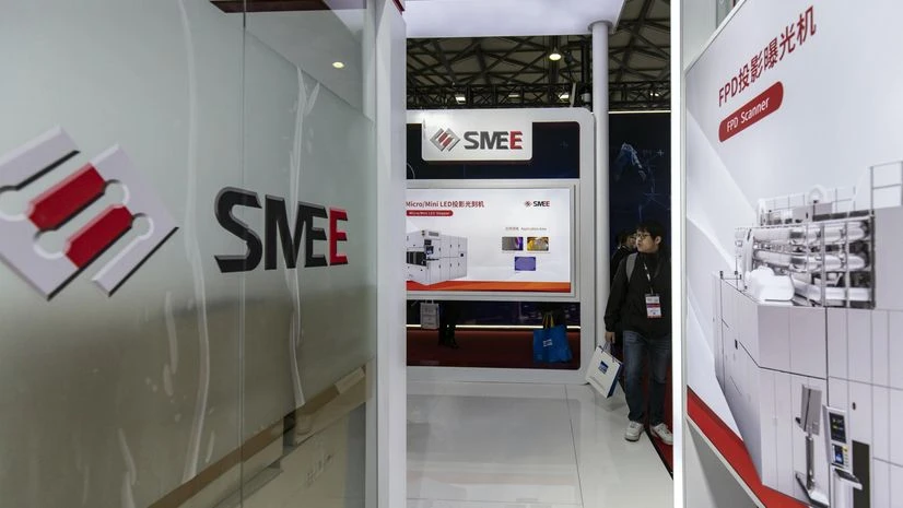
Companies like SMEE are racing to develop machines that can close the gap with suppliers like ASML Holding NV.Photographer: Qilai Shen/Bloomberg
China has claimed a breakthrough in the development of homegrown chipmaking equipment, an important step in overcoming US sanctions designed to thwart Beijing’s semiconductor goals.
State-linked organisations are advised to use a new laser-based immersion lithography machine with a resolution of 65 nanometers or better, the Ministry of Industry and Information Technology said in an announcement this month. Though the note doesn’t specify the supplier, the spec marks a significant step up from the previous most-advanced indigenous equipment — developed by Shanghai Micro Electronics Equipment Group Co. — which stood at around 90nm.
Chipmaking equipment is one of the key bottlenecks in China’s semiconductor ambitions, which the US is trying to contain. Companies like SMEE are racing to develop machines that can close the gap with suppliers like ASML Holding NV, which are now barred from shipping to China. The advances claimed by MIIT last week suggest that homegrown rivals are starting to make headway in developing more sophisticated machines, though SMEE and its peers have a long way to go to catch the likes of ASML.
In its note, the MIIT also named a slew of additional home-developed chip-related gear it wanted to see put into wider use, including oxidation furnaces and dry-etching gear.
While it’s widely believed that China would struggle to move far beyond its current level of sophistication — as exemplified by Huawei’s 7nm Kirin mobile chip introduced a year ago — the lack of transparency has elicited concern in Washington about the effectiveness of its trade curbs.
The Biden administration has implemented sweeping export controls on China and has also pressed the Netherlands for tighter restrictions on ASML’s China business. China relies on ASML’s immersion deep ultraviolet lithography systems to advance its chipmaking technology, as the country has not yet been able to develop similarly capable equipment.
First Published: Sep 16 2024 | 10:39 PM IST


